My (ongoing!) journey to learning PCB design, and making a keypad
WIP, not finished
Hello again, its been a while since ive stared at this grey screen to type about random thing im interested in currently! on tonight’s post, we (i) will be talking about PCB design, what am i doing to learn it, what did i make so far, and what will i (hopefully) make in the future :D
In this post ill quickly share the PCBs ive already designed, and talk about what i did/think i did wrong or right for you to point and laugh, but perhaps learn, after that ill talk about the keypad and how it functions because im really proud of it :)
I will also share resources i found useful at the end of the post (meaning whenever i finish writing it lol), i can’t share pictures of the actual PCBs after manifacturing because.. i haven’t made any of them, costs are too high around here for me to be able to
I will also try add an explination for everything at the very end, so you can follow even if you don’t know much about PCB design/electronics :)
Why am i learning it
Put simply, im an electronics engineering student, and thought it might be a useful skill to have in my field, so why not? resources are (as always) available online and for free, so the only thing i need to spend is some amount of time and a good amount of effort, which im willing to do
Starting small.. too small
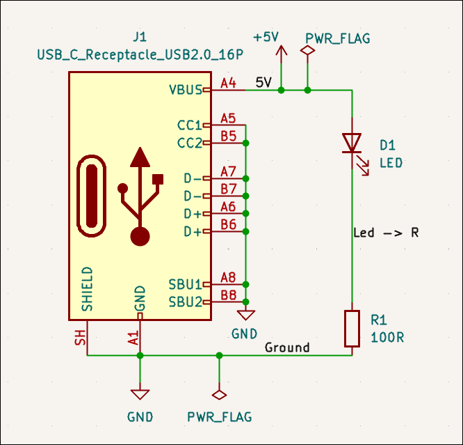
Schematic:
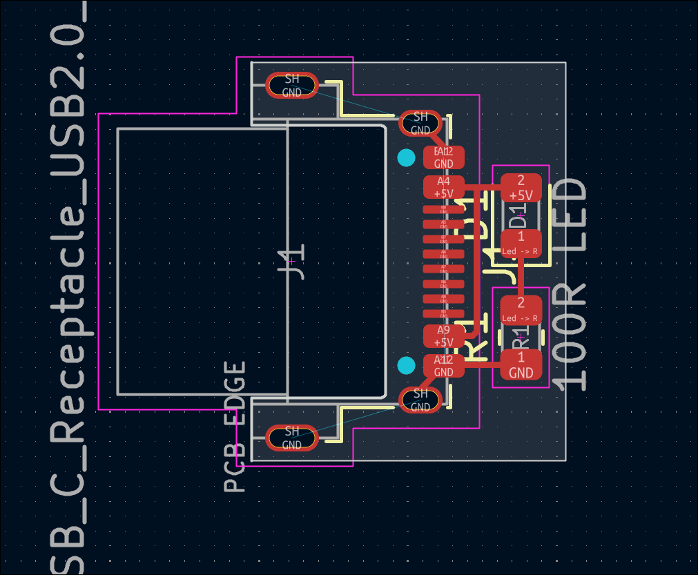
 Layout:
 3D:
3D:
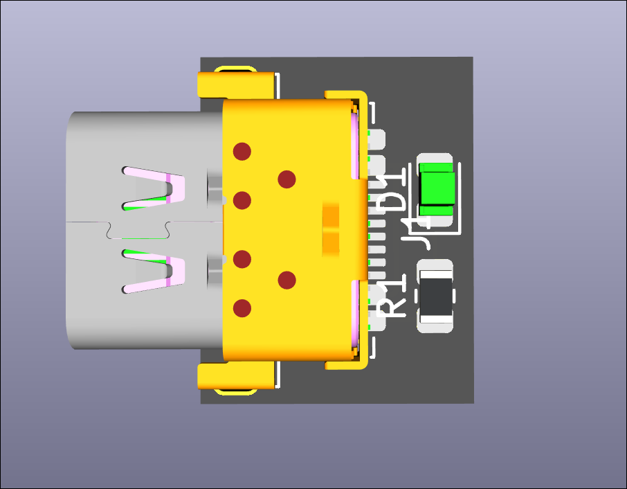
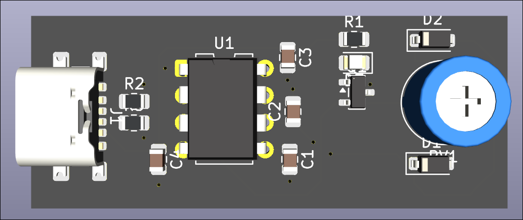
This is my first PCB, as you can not see, its supposed to be a USB-C powered LED, the biggest issue with it is im using whats called a “receptacle”, which in more human terms means its a female port, not a male one, meaning id need a cable to turn the stupid LED on.. i really did start knowing nothing ha
Other smaller problems include using very thin traces for 5v and GND, and connecting the THT wholes of the female port to ground by a trace even tho i should just fill the plane with GND instead and let THAT do the job
Getting more confident
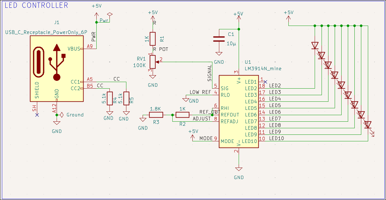
Schematic:
 Front layer:
 Back layer:
 3D:
3D:
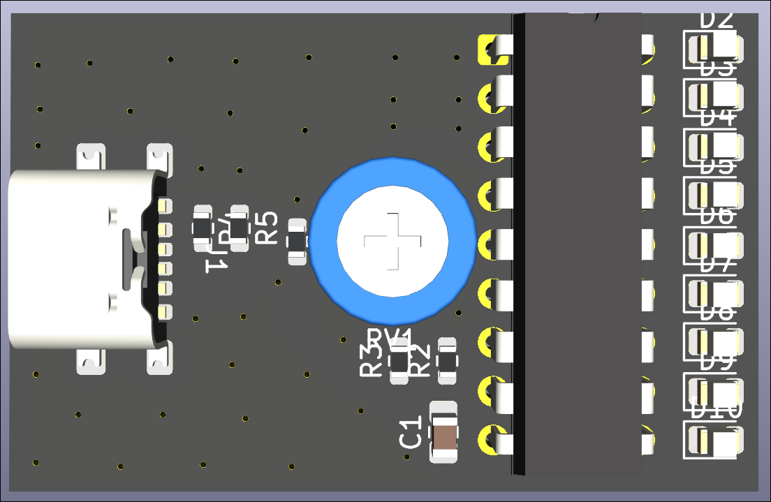
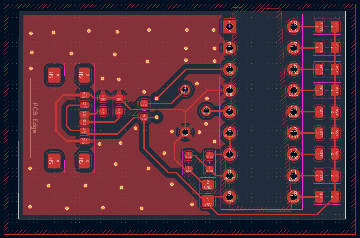
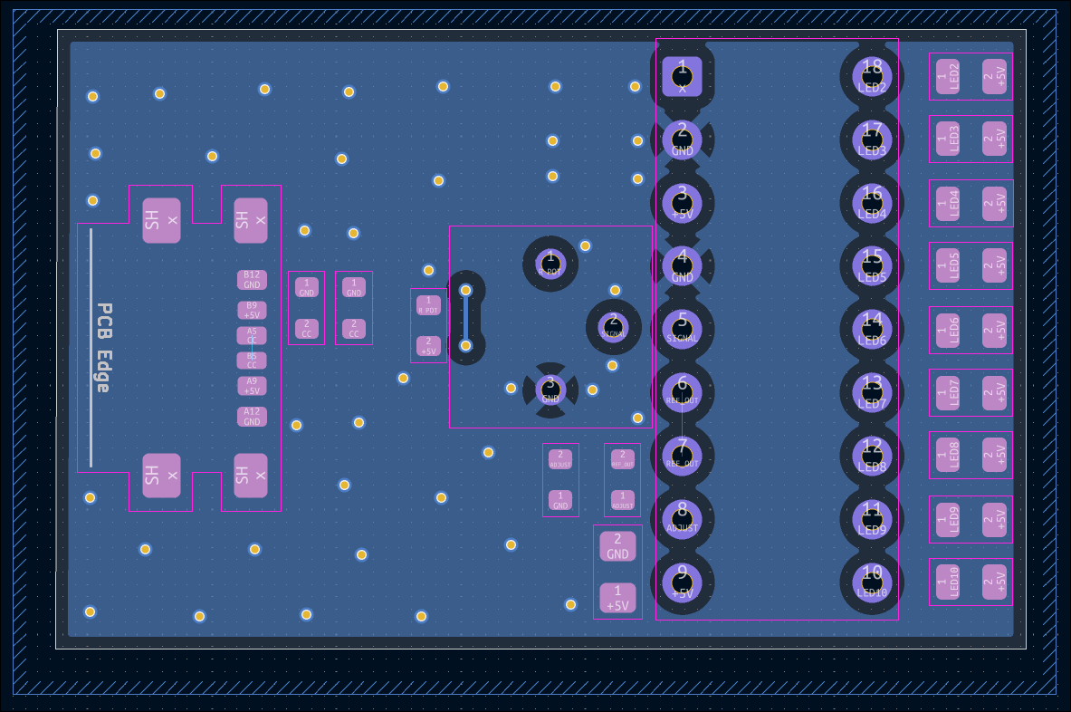
Still on the theme of LEDs for some reason and after a huge amount of youtube tutorials, i made this, which as you can tell (by reading the title on the top left of the box), is an LED controller…… using a potentiometer, should’ve been more descriptive on the title
Anywho, its board that aims to turn on more LEDs the more you turn on the potentiometer, im still not good enough at this to critic my own half decent designs, but i definitely think using very varying values of resistors wasn’t a good idea as it increases manifacturing costs, because these things are too cheap not to sell in bluks of 100s and above. also i should’ve spaced the stitching vias better, and im still using thin traces, also im not sure why i used an annoying SMD pot while
Another project of a similar level
Schematic:
 Front layer (for some reason i forgot to add a copper fill here):
 Back layer:
 3D:
3D:
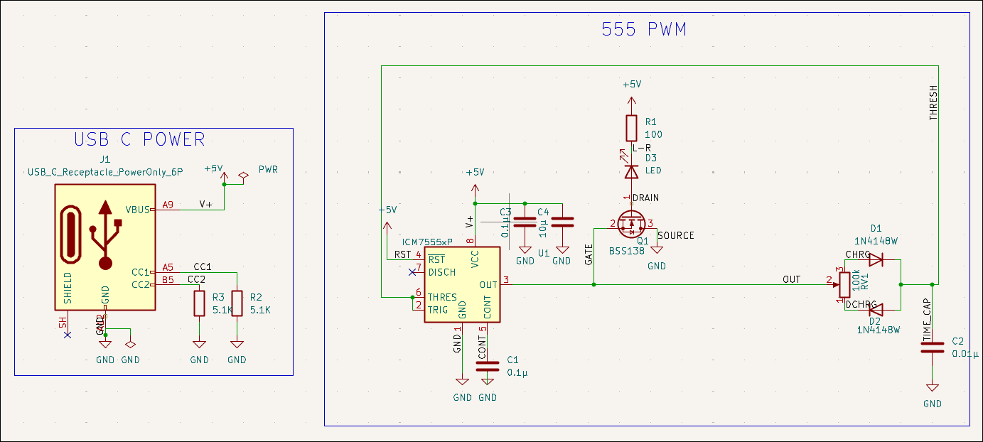
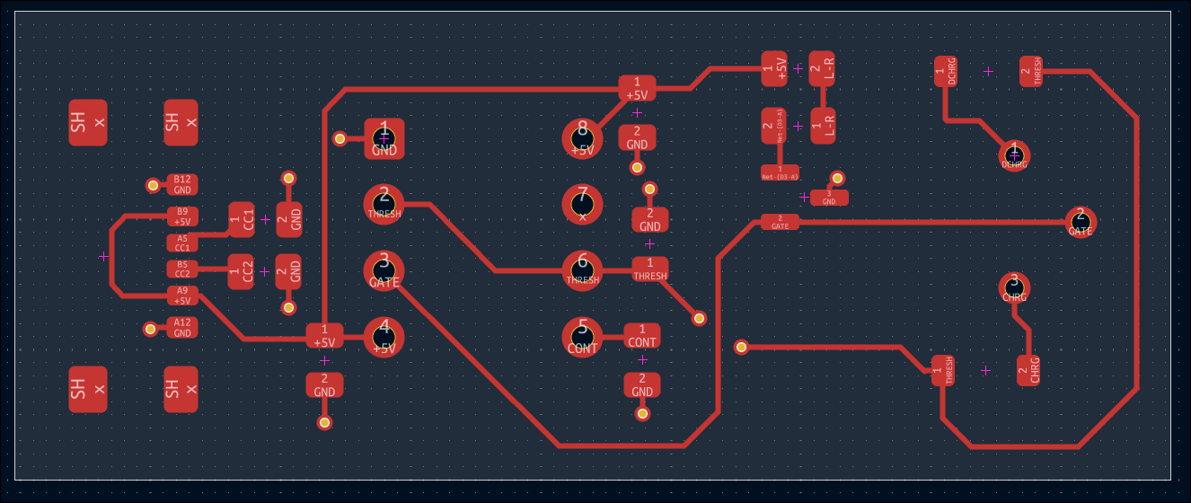
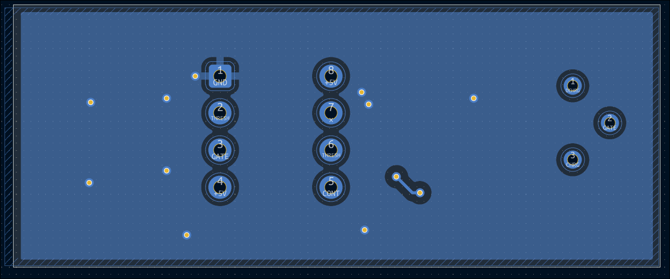
Another LED project, im sure you’re very excited to read about this one! haha.. anyway, in this board, instead of controlling how many LEDs are ON at one time, im controlling how intense a single LED is lighting up using PMW, which this video/post ADD LINK LATER explains better than i ever could
A dev board
Schematic:
 Front layer:
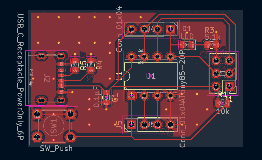 Back layer:
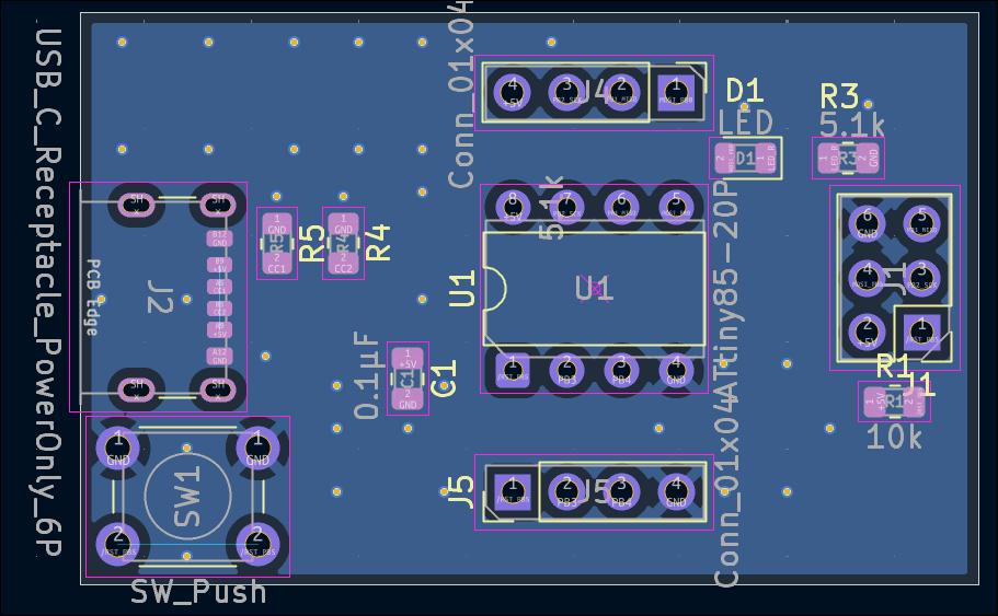 3D:
3D:
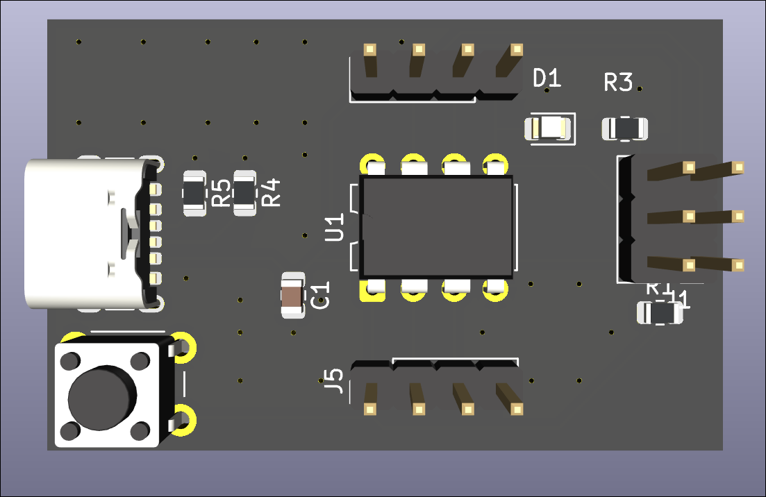
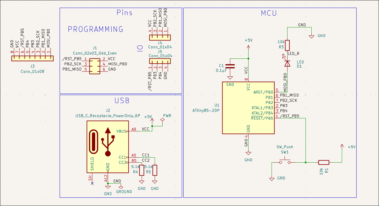
Leaving LEDs behind, i decided to try my hands on making something i already use quite often, an ESP32 dev board! except right now thats way above my level, so instead i lowered the difficulty (a LOT) and made a dev board for the ATtiny-85, which as the name suggets, its pretty tiny, and has a whopping 8 pins, 2 of which are power, making it only necessary to route 6 pins in total, and as per tradition an LED must exist on dev boards, making the total number of useful pins 5
My beloved child
We’ve finally reached the whole point of making this post, the KEYPAD, which is a smaller keyboard used for macros, for example having ctrl+c mapped to one button instead of 2, super simple example obviously, but you get the idea, you can map anything to a button on this keyboard
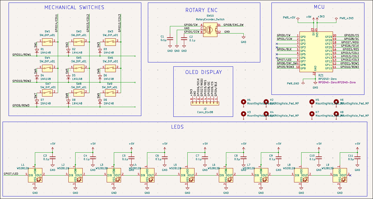
Starting from the left, the matrix of mechanical switches, i learnt how they work from a few youtube videos (i will link them later) and the official QMK docs, if you don’t know QMK it’s an open source firmware used to create custom keyboards, usually mechanical, so their docs are quite useful for a project like this as you can guess. Though i realized later that it might’ve been a better idea to just hook up every indivisual button to a seperate pin of the MCU, since im only using 9 buttons and not building a full keyboard with idk how many buttons, matrices like this save alot of pins but are only useful if pin count is actually a problem, which it isn’t in this case, since for example if you’re making a keyboard with 144 buttons, you would either need 144 indivisual pins OR 12rows * 12columns so only 24 pins saving you a whooping 120 pins. In my case, i saved 0 pins since i need to either hook up 9 indivisual pins or 3rows * 3columns which is still 9 pins…. but hey it was a nice learning experience:)
Going to the rotary encoder, the idea is to have this act as a volume knob, and clicking it mutes the volume, easy and simple does it (INEEDTO EXPLAIN WHY ARE THERE CAPS)
Passing to the OLED display, i had a spare SPI 0.96” display and thought hey it’ll fit right in here, while making it (somewhat) unique, i can display a logo or have preset for the keypad and use the display to show which preset im on, have different mappings for different programs show the current program im using currently, display a cute anime girl face, the possibilities are endless!
For the MCU, i used an RP2040 (more well known as the Raspberry Pi pico), specifically this dev board from Aliexpress, since it’s smaller thus saves space. The only problematic thing about it is the number of pins, but they suffice largely here. I didn’t use a full sized pico just because if i did i would have to drop the buttons a good bit down, which i didn’t wanna do
The mounting hole are for.. mounting. More seriously, there’s 8 because 4 of them are used for mounting the OLED while the other 4 are used for the board itself (you’ll see in the layout/pcb)
The last part of the schematic is the LEDs, which you will notice have capacitors next to them, that’s because these LEDs are quite bright meaning they pull a decent bit of current which can drop the voltage under the forward voltage of these LEDs, we use the caps to provide a short burst of the current which mitigates the issue
With that said and done, lets look at the layout:
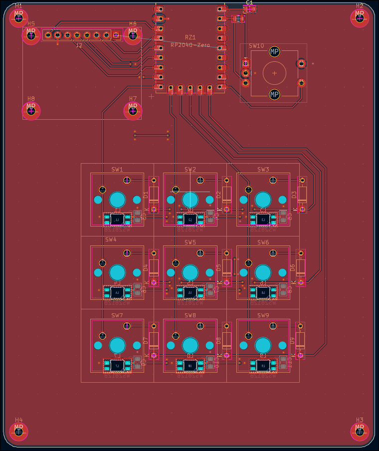
Front layer:
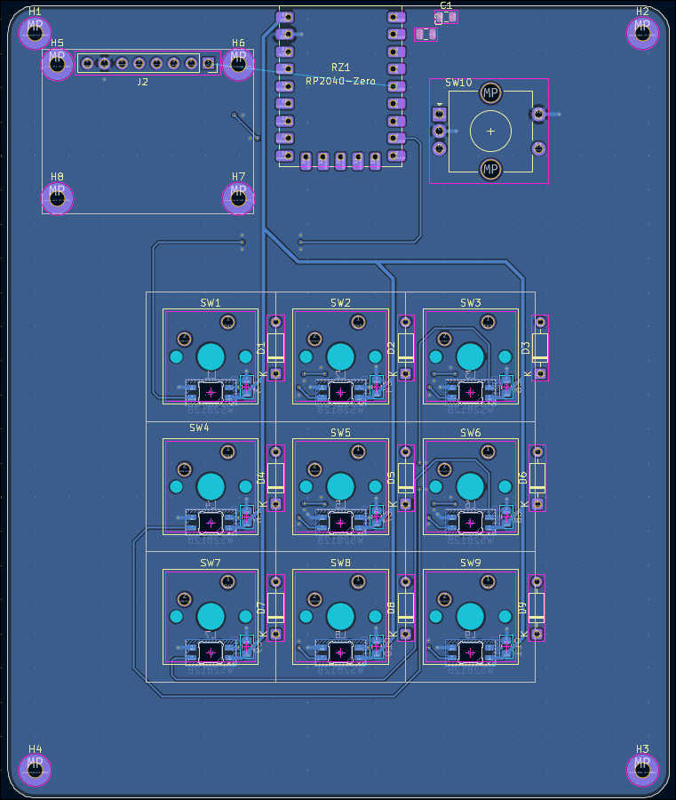
 Back layer:
 Combined:
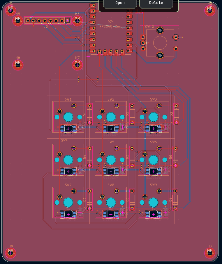
The layout is pretty straightforward, MCU in the top-middle part since that’s where i want the USB-C port to be, to the right we have the encoder since i thought by having this keypad on the right of my desk and having the encoder on the right, it leaves the screen visible and clear of obsticales (the encoder in question, or my hand trying to use said encoder), and the keys being in the middle made the most sense
The LEDs for the keys might look a little weird on the layout, that’s because they are what’s called “reverse mount LEDs” meaning they mount/connect on the back layer of the PCB, but light up on the front layer, which just makes routing and soldering a tiny easier
Two things the keen eyes among you might’ve noticed, one is there’s a missing trace (most right of the OLED display), it’s not needed from i searched and i genuinely could not be bothered if it is needed ill just solder a wire, and second is the use of THT diodes and not SMD that’s simply because that’s what i have atm and i didn’t wanna buy more diodes ill use for one project and never again
The routing is super basic as again im still a beginner, i tried to incorporate a few things i learned as i was making this (i keep trying to learn new things pretty much all the time) such as adding “return path vias” when switching layers, making power traces thicker than signal
Keypad conclusion
That pretty much sums it up for this project, i didn’t bother making a 3D case since (at this moment) i won’t be able to order the PCBs since they’re quite expensive sadly so that’ll have to wait, though i might make it anyways if im ever looking for a new skill to learn aka basic 3D design. It was a fun project, and im happy with how it turned out (virtually), made me learn a bunch of new stuff too which is always welcomed :D
Conclusion
Learning skills is hard and takes time, but at the same time is extremely rewarding (damn am i actually getting decent at writing conclusions???), ill definitely continue learning PCB design as much as i can, especially this summer, hopefully ill reach the point of being able to bring any project idea to life easily, as i certainly can’t right now :)